IBM BlueGene Processors

Introduction
HPC Architecture
  1. Shared-memory SIMD machines
  2. Distributed-memory SIMD machines
  3. Shared-memory MIMD machines
  4. Distributed-memory MIMD machines
  5. ccNUMA machines
  6. Clusters
  7. Processors
    1. AMD Opteron
    2. IBM POWER5+
    3. IBM BlueGene processors
    4. Intel Itanium 2
    5. Intel Xeon
    6. The MIPS processor
    7. The SPARC processors
  8. Networks
    1. Infiniband
    2. InfiniPath
    3. Myrinet
    4. QsNet
    5. SCI
Available systems
  1. The Bull NovaScale
  2. The C-DAC PARAM Padma
  3. The Cray X1E
  4. The Cray XT3
  5. The Cray XT4
  6. The Cray XMT
  7. The Fujitsu/Siemens M9000
  8. The Fujitsu/Siemens PRIMEQUEST
  9. The Hitachi BladeSymphony
  10. The Hitachi SR11000
  11. The HP Integrity Superdome
  12. The IBM eServer p575
  13. The IBM BlueGene/L&P
  14. The Liquid Computing LiquidIQ
  15. The NEC Express5800/1000
  16. The NEC SX-8
  17. The SGI Altix 4000
  18. The SiCortex SC series
  19. The Sun M9000
Systems disappeared from the list
Systems under development
Glossary
Acknowledgments
References

At the time of writing this report two BlueGene types of systems have become available: the BlueGene/L and the BlueGene/P, the successor of the former. Both feature processors based on the PowerPC 400 processor family.

The BlueGene/L processor

This processor is in fact a modified PowerPC 440 processor, which is made especially for the IBM BlueGene family. It runs presently at a speed of 700 MHz. The modification lies in tacking on floating-point units (FPUs)that are not part of the standard processor but can be connected to the 440's APU bus. Each FPU contains two floating-point functional units capable of performing 64-bit multiply-adds, divisions and square-roots. Consequently, the theoretical peak performance of a processor core is 2.8 Gflop/s. Figure 9. shows the embedding of two processor cores on a chip.

Block diagram of an IBM BlueGene/L processor chip

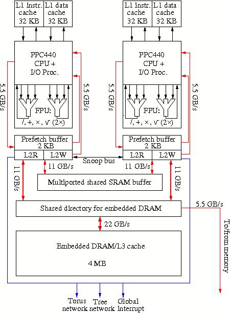
Figure 9: Block diagram of an IBM BlueGene/L processor chip.


As can be seen from the figure the L2 cache is very small: only 2 KB divided in a read and a write part. In fact it is a prefetch and store buffer for the rather large L3 cache. The bandwidth to and from the prefetch buffer is high, 16 B/cycle to the CPU and 8 B/cycle to the L2 buffer. The memory resides off-chip with a maximum size of 512 MB. The data from other nodes are transported through the L2 buffer, bypassing the L3 cache in first instance. The packaging of the 2-CPU nodes in the BlueGene/L is discussed in the section describing the BlueGene systems.

The BlueGene/P processor

Presently little detail is known about the BlueGene/P processor. It is based on the PowerPC 450 at a clock frequency of 850 MHz and with similar floating-point enhancements as applied to the PPC 440 in the BlueGene/L. The BlueGene/P node will contain 4 processor cores which brings the peak speed to 13.6 Gflop/s/node. As yet not many details about memory speed and size, nor the bandwidths between the components on the chip are available: all speeds are about doubled which is necessary because the double amount of cores on the chip. Therefore the bandwidth from memory to an individual core is still 2B/cycle as in the BlueGene/L. Also the L3 size and the memory/core are doubled. The same holds for the network speed in the configuration.