Although the Intel Xeon processors are not applied in integrated parallel systems these days, they play a major role in the cluster community as the mojority of compute nodes in Beowulf clusters are of this type. Therefore we briefly discuss also this type of processor. We concentrate on the Xeon, the server version of the IA-32 processor family, as this is the type to be found in clusters, mostly in 2-processor nodes.
As of 2006 Intel has introduced an enhanced microarchitecture for the IA-32 instruction set architecture called the Core architecture. The server version with the code name Woodcrest is a first implementation of this new microarchitecture. The Woodcrest processor has two processor cores as now all high-end processors do. In addition, many improvements have been made to increase the performance and at the same time to decrease the power requirements. In November 2007 Intel has introduced a quad-core processor, code name Clovertown. In fact it features to two Woodcrest processors on one chip which all share the 1333 MHz frontside bus to the memory (maximum, also 1066 MHz FSB variants are offered). In the following we discuss mostly the Woodcrest structure as this is essentially the same as for the quad-core Clovertown. A fairly extensive evaluation of the latter can be found (see 47).
In Figure 12 a block diagram of a Woodcrest processor is shown with one of the cores in some detail. Note that the two cores share one second level cache while the L1 caches and TLBs are local to each of the cores
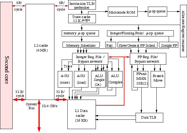
Figure 12: Block diagram of the Intel Xeon processor.
while the connection to the memory via the off-chip memory controller is depicted in Figure 12a
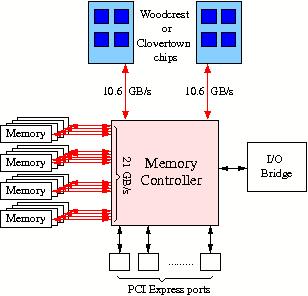
Figure 12a: Diagram of the connection of the memory to Woodcrest or Clovertown processors.
To stay backwards compatible with the x86 (IA-32) Instruction Set Architecture which comprises a CISC instruction set Intel developed a modus in which these instructions are split in so-called micro operations (µ-ops) of fixed length that can be treated in the way RISC processors do. In fact the µ-ops constitute a RISC operation set. The price to be payed for this much more efficient instruction set is an extra decoding stage.
Many of the improvements of the Core architecture are not evident from the block diagram. For instance in the Core architecture 4 µ-ops/cycle can be scheduled instead of 3 as in the former microarchitecture. Futhermore, some macro-instructions as well as some µ-ops can be fused, resulting in less instruction handling, easier scheduling and better instruction throughput because these fused operations can be executed in a single cycle.
As can be seen in Figure 12 the processor cores have an execution trace cache which holds partly decoded instructions of former execution traces that can be drawn upon, thus foregoing the instruction decode phase that might produce holes in the instruction pipeline. The allocator dispatches the decoded instructions, the µ-ops, to the appropriate µ-op queue, one for memory operations, another for integer and floating-point operations.
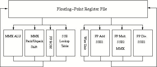
Figure 12b: Intel Xeon floating-point unit.
Two integer Arithmetic/Logical Units are kept simple in order to be able to run them at twice the clock speed. In addition there is an ALU for complex integer operations that cannot be executed within one cycle. The floating-point units, depicted in Figure 12b, contain also additional units that execute the Streaming SIMD Extensions 2 and 3 (SSE2/3) repertoire of instructions, a 144-member instruction set, that is especially meant for vector-oriented operations like in multimedia, and 3-D visualisation applications but which will also be of advantage for regular vector operations as occur in dense linear algebra. The length of the operands for these units is 128 bits. The throughput of these SIMD units has been increased by a factor of 2 in the Core architecture which greatly increase the performance of the appropriate instructions. The Intel compilers have the ability to address the SSE2/3 units. This makes it in principle possible to achieve a 2–3 times higher floating-point performance.
The Xeons boast so-called Hyperthreading: with the processor two threads can
run concurrently under some circumstances. In this it is not unique anymore as
all main processor makers now provide some form of multi-threading. It may for
instance be used for speculative execution of if branches. Experiments
have shown that up to 30% performance improvements can be attained for a
variety of codes. In practice the performance gain about 3–5%, however.
The secondary cache has a size of 4 MB for the Woodcrest implementation of the
Core processor. The two core share a forntside bus with a bandwidth of 10.6
GB/s.
Since its predecessor, the Nocona processor the Intel processors have the ability to run (and address) 64-bit codes, thereby following AMD, in fact copying the approach used in the AMD Opteron and Athlon processors. The technique is called Extended Memory 64 Technology (EM64T) by Intel. In principle it uses "unused bits" from in the instruction words of the x86 instruction set to signal whether an 64-bit version of an instruction should be executed. Of course some additional devices are needed for operating in 64-bit mode. These include 8 new general purpose registers(GPRs), 8 new registers for SSE2/3 support, and 64-bit wide GPRs and instruction pointers.
As in the dual-core Montecito (see Itanium 2) We do
not show that in a separate figure as the configuration is very similar to that
in the Montecito.
It will depend heavily on the quality of the compilers whether they will be able
to take advantage of all the facilities present in the dual-core processor.