The Opteron dual core processor is the currently most common part of the AMD Opteron family. It is manufactured in 90 nm feature size (65 nm coming up shortly) and available since the end of 2005. It is a clone with respect to Intel's x86 Instruction Set Architecture, and it is quite popular for use in clusters. In addition it is used in Cray and the "Barcelona" will come onto the market shortly but it is not yet available at the time of writing this report. The cores in the Barcelona chip will have double the floating-point units that are present in the current processor cores. As we do not have sufficient detail yet on the Barcelona chip we only discuss the dual core Opteron here.
As already mentioned, the Opteron processor has many features that are also present in modern RISC processors: it supports out-of-order execution, has multiple floating-point units, and can issue up to 9 instructions simultaneously. In fact, the processor core is very similar to that of the Athlon processor. A block diagram of the processor is shown in Figure 7
Note that in the dual core version two of these cores are housed on one CPU chip. The two cores are connected by an on-chip crossbar (see next section) that also connects to the memory controller and to other processors on the board (if present).
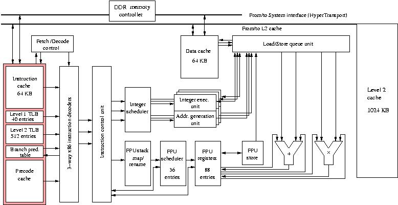
Figure 7: Block diagram of an AMD Opteron processor core.
The Figure shows that the processor has three pairs of Integer Execution Units and Address Generation Units that via an 24-entry Integer Scheduler takes care of the integer computations and address calculations. Both the Integer Scheduler and the Floating-Point Scheduler are fed by the 96-entry Instruction Control Unit that receives the decoded instructions from the instruction decoders. An interesting feature of the Opteron is the pre-decoding of x86 instructions in fixed-length macro-operations, called RISC Operations (ROPs), that can be stored in a Pre-decode Cache. This enables a faster and more constant instruction flow to the instruction decoders. In comparison to the Athlon the instruction decode pipeline has been deepened by two stages to 12 to enable a higher yield of ROPs. Like in RISC processors, there is a Branch Prediction Table assisting in branch prediction.
The floating-point units allow out-of-order execution of instructions via the FPU Stack Map & Rename unit. It receives the floating-point instructions from the Instruction Control Unit and reorders them if necessary before handing them over to the FPU Scheduler. The Floating-Point Register File is 88 elements deep which approaches the number of registers as is available on RISC processors. (For the x86 instructions 16 registers in a flat register file are present instead of the register stack that is usual for Intel architectures.)
The floating-point part of the processor contains three units: a Floating Store unit that stores results to the Load/Store Queue Unit and Floating Add and Multiply units that can work in superscalar mode, resulting in two floating-point results per clock cycle. Because of the compatibility with Intel's Pentium III processors, the floating-point units also are able to execute Intel SSE2/3 instructions and AMD's own 3DNow! instructions. However, there is the general problem that such instructions are not directly accessible from higher level languages, like Fortran 90 or C(++). Both instruction sets are meant for massive processing of visualisation data.
Due to the shrinkage of components the chip now can harbour the secondary cache of 1024 KB with an 8-cycle latency and the memory controller. This, together with a significantly enhanced memory bus can deliver up to 6.4 GB/s of bandwidth, an enormous improvement over the former memory system. This memory bus, called HyperTransport by AMD, is derived from licensed Compaq technology and similar to that employed in Compaq's former EV7 processors. It allows for "glueless" connection of several processors to form multi-processor systems with very low memory latencies. HyperTransport 1, the present bus, can transport 8 GB/s, including cache coherency traffic, I/O, and interprocessor data.
The clock frequency is in the range of 2.2–2.8 GHz which makes the Opteron an interesting alternative for the few RISC processors that are still available at this moment. Especially the HyperTransport interconnection possibilities makes it highly attractive for building SMP-type clusters. A very large (over 11,000 processor) Opteron cluster, the Red Storm system, has been built at Sandia National Laboratory by Cray Inc. which uses the HyperTransport facility because it is an open standard that makes the connection with the Cray network much simpler. The same principle is used in its commercial offspring, the Cray XT3 and XT4.