Quite unexpectedly the MIPS processor has turned up again in the HPC area because it is employed in SiCortex machines, see the section on the SciCortex. The last time a MIPS processor featured in an HPC system it was the R14000 variant that populated the SGI Origin 3000 series. Now it is back not because it is particularly fast but because of its very low power requirement at the clock frequency that is used: 500 MHz. The processor looks very much like the late R14000 processor and as such is a typical representative of simple straight-forward RISC processors. A block diagram is shown in Figure 13.
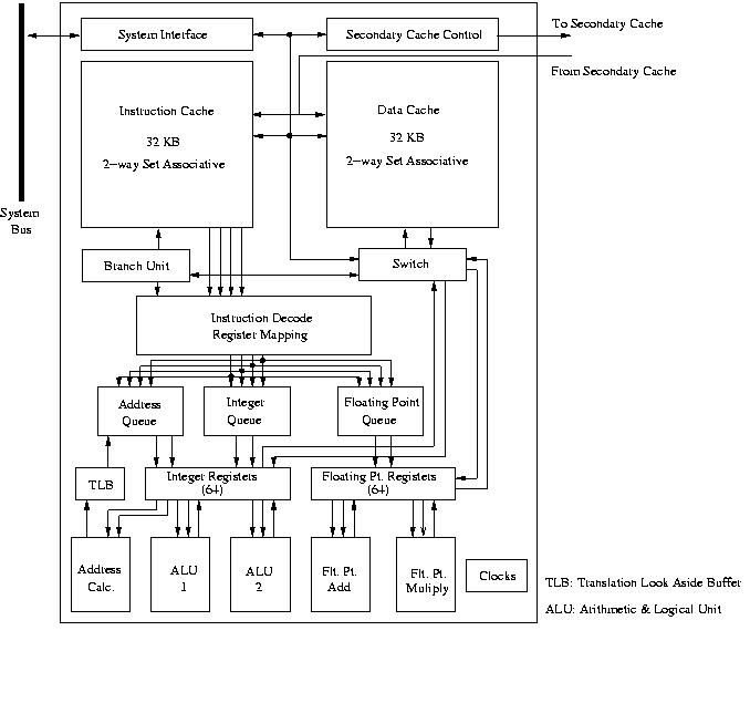
Figure 13: Block diagram of a MIPS processor.
There are two independent floating-point units for addition and multiplication and, additionally, two units that perform floating division and square root operations (not shown in Figure 13). The latter, however, are not pipelined and with latencies of about 20–30 cycles are relatively slow. In all there are 5 pipelined functional units to be fed: an address calculation unit which is responsible for address calculations and loading/storing of data and instructions, two ALU units for general integer computation and the floating-point add and multiply pipes already mentioned.
The level 1 instruction and data caches have a moderate size of 32 KB and are 2-way set-associative. In contrast, the secondary cache can be very large: up to 16 MB but in the system they are now employed in the it has a 256 KB section in a 1.5 MB shared L2 cache. Both the integer and the floating-point registers have a physical size of 64 entries, however, 32 of them are accessible by software while the other half is under direct CPU control for register re-mapping.
As already remarked, the clock frequency of the processor is quite low, 500 MHz and therefore the theoretical peak performance is 1 Gflop/s. This is not all bad. It has in fact chosen to be that low intentionally in order to have a very low power dissipation: only slightly less than 1 Watt. To achieve this the processor design had to be somewhat simplified in comparison to the former Rx000 series of processors. The instruction execution is done in-order which potentially can lower the number of instructions that can be processed per cycle. On the other hand, the discrepancy between the processor speed and the memory speed is much smaller than in other processors which leads to a higher average efficiency. Especially in codes with irregular but intensive memories access patterns the actual speed per processor might not be very much slower than experienced on other systems because of this smaller memory gap.